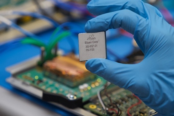
SANTA CLARA, Calif. –October 9, 2024 – Eliyan Corporation, credited for the invention of the semiconductor industry’s highest-performance and most efficient chiplet interconnect, today revealed the successful delivery of first silicon for its NuLink™-2.0 PHY, manufactured in a 3nm process. The device achieves 64Gbps/bump, the industry’s highest performance for a die-to-die PHY solution for multi-die architectures. While compatible with UCIe standard, the milestone further confirms Eliyan’s ability to extend die-to-die connectivity by 2x higher bandwidth, on standard as well as advanced packaging, at unprecedented power, area, and latency.
The NuLink-2.0 is a multi-mode PHY solution that also supports UMI (Universal Memory Interconnect), a novel chiplet interconnect technology that improves Die-to-Memory bandwidth efficiency by more than 2x. UMI leverages a dynamic bidirectional PHY whose specifications are currently being finalized with the Open Compute Project (OCP) as BoW 2.1.
The NuLink-2.0 demo vehicle uses standard organic/laminate packaging with 5-2-5 and 8-2-8 stack ups. The highly area efficient NuLink PHY is bump limited and fits not only under 90um bump pitch in standard packaging, but also under 45-55um bump pitches in advanced packaging. It can deliver bandwidth of up to 5Tbps/mm in standard packaging by leveraging innovative reflection and crosstalk cancellation techniques, and up to 21Tbps/mm in advanced packaging at reduced power by leveraging unterminated receivers and simplifying the cancellation circuitry. NuLink’s unprecedented low power makes it an ideal PHY solution that meets the stringent power density requirement of custom HBM4 base die, which is a critical piece of all future AI systems.
The device includes a die-to-die PHY coupled with an adaptor/link layer controller IP to provide a complete solution, aligned with the high-growth AI markets for HPC and edge applications. Lower costs accommodated by utilizing standard packaging can further encourage chiplet-based designs in inference and gaming segments, as well as other adjacent markets as they can be more readily qualified for aerospace, automotive, and demanding industrial markets.
“This milestone sets a new standard in Perf/TCO advantages for implementing a wide range of multi-die use cases,” said Eliyan’s founding CEO Ramin Farjadrad. “The performance alone expands the degrees of freedom for architects working to remove or lessen memory and IO walls. Combined with unprecedented low power consumption and flexibility in packaging technology for market-specific optimization around cost and complexity, we are able to deliver a solution that will help scale chiplet-based design to new levels of capabilities in a diverse range of industries.”